Manufacturing Services

Printed Circuit Board Loading

Small Volumes Accepted

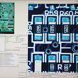
Loading a PCB typically involves three different areas with different methods of component preparation and different placement techniques.

PCB's designed for production are generally cheaper to manufacture than boards requiring excessive manual intervention. If unsure about production ready PCBs then please contact us for general advice.

PCB Loading Methods

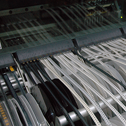
  • Surface Mount placement is the most common design used today. This involves placing reels of components on a Pick and Place Machine and configuring that machine to place the component in its designated spot.
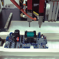
  • Through Hole placement generally involves the pre-preparation of the component for insertion into the PCB. Typical preparation involves lead forming and bending the component.
  • Finally there is the Custom Component. Today components are becoming varied and complex, with specialized placement techniques. These components generally require manufacturer's special instructions for placement.

Soldering Methods

  • Surface Mount components are placed onto solder paste deposited on the PCB and then sent though an oven with an individual soldering profile.
  • Through Hole components are typically soldered on a wave soldering machine but are also hand soldered if they are in a difficult position on the PCB.
  • Custom components may use either of the above techniques or be press-fitted or use some other special technique.

Automatic Optical Inspection (AOI)

Inspects Solder Joints & Component Identification

Our Automatic Optical Inspection (AOI) uses a 3-CCD color camera and other cameras to visually inspect a wide range of defects on a PCB. Typical defects might include dimensional defects such as insufficient solder, solder bridges, missing solder, missing or incorrectly placed components.

Component identification is the second important task performed by AOI. The marking of each component is verified against a database of component markings. The database is constantly expanded to include varying markings from different manufacturers of the same component.

Golden Board

  • Each production run of PCBs is compared to a Customer supplied Golden Board
  • All Golden Boards are tracked by Version Numbers
  • AOI provides Production Batch manufacturing verification

AOI is not to be confused with Testing

  • Successful AOI outcomes do not guarantee a functioning board
  • Only Board Testing can verify the validity of component performance

PCB Board Testing

Full ICT / MDA Service

In-Circuit Testing (ICT) involves the use of a bed of nails jig to gain access to various nodes on an assembled Printed Circuit Board so that a variety of tests may be performed on the assembly. Tests include integrity of tracks, measurement of resistance and capacitance along with many other measurements.

After testing is performed and the board is electrically sound, the next stage involves loading firmware into various components thus bringing the assembly to life. Once concluded, the ICT can start to perform live test on many parts of the assembly.

ICT must be designed in

  • ICT must be considered at the start of design
  • Test points must be accessible by probes
  • Consider test points for functional live test
  • Test jigs can measure colour & intensity of LEDs
  • Many tests are possible on our ICT machine

Conformal Coating

Selective and Accurate

Conformal coating of PCBs is normally required when the assembly is destined for a harsh environment. The two typical methods of conformal coat are by spraying or dipping. Often dipping is not possible because the PCB contains connectors which must not be coated.

This is where our conformal coating machine becomes a more versatile option. Software is used to select sections of a PCB to be sprayed. The spraying is then with special spray heads at extremely low PSI settings, this eliminates any overspray to neighbouring components.

Considerations

  • There are different types of Conformal Coat for varied applications
  • Consider which product is suitable for your application
  • Consider which parts of your PCB need to be protected
  • Thicker applications are achieved by multiple spray passes
  • Some conformal coats contain a UV tracer for application verification

Ultrasonic Welding

Product Welding

Welding thermoplastic materials by means of ultrasonics has quickly become an established method, thanks to the continuous development of the plastics trade and the clean, simple application of this technology. The ultrasonic welding enables a safe and above all long-living connection of different products. The feature of a permanent joint – i.e. the conscious decision to forfeit the option of future disassembly and repair – for common consumer products, has also contributed. Another important area of application is the manufacturing of disposable products for hygienic purposes, for example in the field of medicine.

Our Equipment

  • We use a Branson 2000 Ultrasonic Welder at our Ringwood factory
  • The process requires a custom product 'nest'
  • The 'nest' is then attached to the machine
  • Custom machine settings are then set for each individual 'nest'
  • The welding operation takes less than a second
  • The finished product becomes tamper proof

Low Melt Overmoulding

Electronics Encapsulation

Low Melt Overmoulding is a simple method of waterproofing electronic assemplies and also providing mechanical support and strain relief. The moulding polyamide-based hot-melt adhesives have a melting range of 120°C to 180°C and are low viscosity and present good adhesion to many plastics such as polyethylene, polyvinyl chloride and polyamide.

The process is related to injection moulding where heated hot-melt adhesive is injected into a tool. The thin molten mass will flow around filigree components at low pressure unlike the high pressure required for conventional plastic injection moulding. The low pressure makes the entire process economical, as both the machine and the tool can be designed for these low loads, allowing the use of inexpensive aluminium tooling.

Advantages

  • Low temperatures will not affect electronic components
  • Encapsulation is both waterproof and tamperproof
  • Electronic Circuits can be encapsulated into a single cable
  • Inexpensive tooling makes low volume possible